Advanced Program
International Symposium on Ultra-parallel Optoelectronics
February 3-4, 2000
Kanagawa Science Park Hall, Kawasaki, Japan
Sponsored by
COE Program "Ultra-Parallel Optoelectronics"
of Ministry of Education, Science, Sports & Culture
&
P & I Lab., Tokyo Institute of Technology
Registration Deadline: January 24, 2000
| Steering Committee: |
|---|
| K. Iga, Tokyo Institute of Technology (Chair) |
| S. Arai, Tokyo Institute of Technology |
| M. Asada, Tokyo Institute of Technology |
| M. Watanabe, Tokyo Institute of Technology |
| T. Baba, Yokohama National Univ. |
| F. Koyama, Tokyo Institute of Technology (Secretary) |
| T. Miyamoto, Tokyo Institute of Technology (Secretary) |
| Advisory Members: |
|---|
| Y. Arakawa | | Univ. of Tokyo |
| T. Ikegami | | Aizu Univ. |
| K. Kobayashi | | NEC |
| M. Nakamura | | Hitachi |
| Y. Suematsu | | Kouchi Univ. of Technology |
| H. Takanashi | | Fujitsu Labs. |
|
|
Scope:
The opto-electronics field is meeting an evolutionary stage, i.e., multi-media networks require a high speed and low cost lightwave infrastructure, and optical Giga-bit Ethernets are penetrating into high speed LAN. Also Giga-byte optical storage systems have begun to be considered. The vertical cavity surface emitting laser (VCSEL) is opening up a new development of such new optoelectronics technical fields.
The International Symposium on Ultra-Parallel Optoelectronics will be held by the following schedule;
Location: Kanagawa Science Park Hall, Kawasaki-shi, Japan
Date: February 3 - 4, in the Year of 2000
This international symposium is sponsored by COE (Center of Excellence) program of Ministry of Education, Science, Sports & Culture. We have been holding the conference series "Semiconductor Laser Symposium" every year for these 15 years. As a special event of this conference series, we have planned this International Symposium in the year of 2000 to conclude the COE Program "Ultra-Parallel Optoelectronics".
The objective of this symposium is to provide a forum for presenting and discussing the recent achievements and important issues related to parallel optoelectronics. The symposium consists of invited papers and contributed poster papers on latest technologies of surface emitting and microcavity lasers, and recently recognized existing topics of optical systems, such as WDM, high-speed LAN, optical storage, information processing, and so on. Speakers in both the device and applications area will be invited to make presentations that highlight recent breakthroughs in this field. Participants would be able to discuss the latest achievements in this field.
Topics:
- Vertical cavity surface emitting lasers (VCSELs) and arrays
- New materials and process technologies for optoelectronic devices
- Micro-cavities and photonic crystals
- Integration and new functions of 2-D arrayed devices
- Applications of VCSELs
- Parallel optical systems (LAN, Interconnects, Optical memories, Information Processing, Sensing, and so on)
- WDM devices and components
Official Language:
The official language of the Symposium will be English, which will be used for all printed materials, presentations, and discussions.
Equipments for Presentation: (for presenters)
Oral presentations: overhead projector, video projector (Please prepare your own computer) are available.
Poster presentations: 180 cm wide x 90 cm high bulletin board (Sticking material is prepared by the committee. adhesive tape only, no pins)
Registration:
The registration fee for the symposium is free, but pre-registration is requested. Send an email containing Name, Affiliation, complete return address, telephone number, facsimile number and e-mail address to <fmatsuna@pi.titech.ac.jp> by January 24, 2000. The total capacity of regisration is 150. The registration arriving first up tofirst up to 150 can only be accepted even no later than the deadline.
Advance Program
February 3 (Thursday)
Opening Session 9:30-10:00 (Chair: S. Arai)
Session A 10:00-12:00 (Chair: J. Jewell and K. Kobayashi)
- A-1
- L. A. Coldren (University of California, Santa Barbara, USA)
High-efficiency epitaxial VCSEL technology
- A-2
- K. J. Ebeling (Ulm University, Germany)
Low noise high speed VCSELs and arrays for optical interconnects
- A-3
- P. D. Dapkus (University of Southern California, USA)
VCSELs and microcavities for parallel processing
- A-4
- D. G. Deppe (University of Texas at Austin, USA)
Vertical cavity surface emitting lasers (VCSELs) and arrays
Session B 13:30-15:30 (Chair: L. A. Coldren and Y. H. Lee)
- B-1
- Y. Arakawa (University of Tokyo, Japan)
Progress in quantum dots for optoelectronics devices
- B-2
- M. Osinski (University of New Mexico, USA)
Design of InGaN/GaN/AlGaN VCSELs using the effective frequency method
- B-3
- N. Ueki, H. Nakayama, J. Sakurai, A. Murakami, H. Otoma, Y. Miyamoto, M. Yamamoto, R. Ishii, M. Yoshikawa, and T. Nakamura (Fuji Xerox, Japan)
Fabrication and property of large scale 2-D VCSEL array
- B-4
- C. Chang-Hasnain (University of California, Berkeley, Bandwidth9, USA)
Wavelength-engineering in VCSELs
Session C 16:00-18:00 (Chair: Y. Arakawa and K. D. Choquette)
- C-1
- Y. H. Lee (KAIST, Korea)
2-dimensional photonic bandgap nano-laser
- C-2
- S. Arai, N. Nunoya, M. Nakamura, H. Yasumoto, and S. Tamura (Tokyo Institute of Technology, Japan)
1.5 µm wavelength GaInAsP/InP low threshold current lasers by low-damage CH4/H2-RIE and OMVPE regrowth
- C-3
- T. Baba, M. Fujita, and A. Sakai (Yokohama National University, Japan)
Microdisk-based photonics
- C-4
- C-4 M. Wu (University of California, Los Angels, USA)
Micromechanical photonic integrated circuits
February 4 (Friday)
Session D 9:00-10:30 (Chair: D. G. Deppe and M. Wu)
- D-1
- N. Yokouchi and A. Kasukawa (Furukawa Electric, Japan)
850nm-VCSELs for high speed datacom applications
- D-2
- K. D. Choquette (Sandia National Laboratory, USA)
High performance 2-dimensional VCSEL arrays for interconnect and imaging applications
- D-3
- K. Takaoka, M. Ishikawa, and G. Hatakoshi (Toshiba, Japan)
InGaAlP-based red VCSELs for high-speed POF data links
Session E 11:00-12:30 (Chair: P. D. Dapkus and M. Osinski)
- E-1
- C. Amano, T. Kagawa, H. Uenohara, K. Tateno, O. Tadanaga, T. Nakahara, H. Tsuda, and Y. Ohiso (NTT, Japan)
Recent activities for VCSELs and related studies in NTT Labs.
- E-2
- M. Kondow, T. Kitatani, and T. Tanaka (RWCP Hitachi Lab., Japan)
GaInNAs for VCSELs
- E-3
- T. Anan, M. Yamada, K. Kurihara, K. Nishi, K. Tokutome*, A. Kamei, and S. Sugou (RWCP NEC Lab., Japan)
GaAsSb-based long-wavelength VCSELs
Session F 14:00-15:30 (Chair: K. J. Ebeling and C. J. Chang-Hasnain)
- F-1
- J. Jewell (PicoLight, USA)
High-performance commercial VCSELs
- F-2
- H. K. Shin (Opticis Corp., Korea)
Optical interface using VCSEL array
- F-3
- K. Iga (Tokyo Institute of Technology, Japan)
Surface emitting laser -its past, present and future-
Poster Session G 16:00-18:00
- Wide-gap Materials and Visible LEDs
- P-1
- M. Iwata, T. Sakaguchi, Y. Moriguchi, Y. Uchida, T. Miyamoto, F. Koyama, and K. Iga (Tokyo Inst. of Tech., Japan)
GaInN multiquantum wells with AlGaN barriers
- P-2
- Y. Moriguchi, T. Miyamoto, T. Sakaguchi, M. Iwata, Y. Uchida, F. Koyama, and K. Iga (Tokyo Inst. of Tech., Japan)
GaN polycrystal light emitter grown on Silica substrate by metalorganic vapor phase epitaxy (MOVPE)
- P-3
- Y. Ishihara, J. Yamamoto, M. Kurimoto, T. Takano, T. Honda, and H. Kawanishi (Kohgakuin University, Japan)
Relationship between XRD peak and residual strain in AlN grown on (0001)6H-SiC by MOVPE
- P-4
- M. Kurimoto, K. Suzuki, Y. Ishihara, J. Yamamoto, T. Takano, T. Honda, and H. Kawanishi (Kohgakuin University, Japan)
Composition fluctuation in AlGaN layers grown by low-pressure metal-organic vapor phase epitaxy
- P-5
- N. Nakada, M. Nakaji, H. Ishikawa, T. Egawa, T. Jimbo, and M. Umeno (Nagoya Institute of Technology, Japan)
InGaN light emitting diode with GaN/AlGaN distributed Bragg reflector
- P-6
- T. Takada, I. Nomura, S. Che, A. Kikuchi, K. Shimomura, and K. Kishino (Sophia University, Japan)
Application of Wide-gap and high-p-dopable BeZnTe II-VI compounds on InP substrates for visible light emitting diodes as p-cladding layers
- GaAs-based VCSELs
- P-7
- N. Nishiyama, S. Shinada, M. Arai, F. Koyama and K. Iga (Tokyo Inst. of Tech., Japan)
Single mode and stable polarization GaInAs/GaAs surface emitting laser grown on GaAs (311)B substrate
- P-8
- Y. Kaneko, D. E. Mars, S. Nakagawa, Y. Ichimura, T. Takeuchi, and N. Yamada (Agilent Laboratories, Japan)
Comparisons for vertical-cavity surface-emitting lasers grown on (311)B and (411)A GaAs substrates
- P-9
- W.-Y. Cho, K.-H. Ha, S. Kim, and W.-L. Hwang (Samsung Electronics, Korea)
Continuous wave operation of 650 nm AlGaInP vertical cavity surface emitting lasers
- P-10
- O. Tadanaga, K. Tateno, H. Uenohara, T. Kagawa and C. Amano (NTT, Japan)
Polarization characteristics of 850 nm InAlGaAs strained quantum-well vertical cavity surface emitting lasers grown on GaAs (311)B substrates
- Novel Long Wavelength Materials and Lasers
- P-11
- D. Schlenker, Z. Chen, M. Kawaguchi, T. Kondo, E. Gouardes, T. Miyamoto, F. Koyama, and K. Iga (Tokyo Inst. of Tech., Japan)
1.2 µm highly strained GaInAs-GaAs quantum well lasers
- P-12
- S. Sato (Ricoh, Japan)
High-performance 1.3 µm range GaInNAs lasers grown by MOCVD
- P-13
- T. Kageyama, T. Miyamoto, S. Makino, N. Nishiyama, F. Koyama, and K. Iga (Tokyo Inst. of Tech., Japan)
GaInNAs/GaAs Quantum well lasers grown by chemical beam epitaxy
- P-14
- M. Takahashi, A. Moto, S. Tanaka, T. Tanabe, S. Takagishi, T. Katsuyama, and A. Ishida (Sumitomo Electric, Japan)
Temperature characteristics of GaInNAs/GaAs quantum well lasers
- P-15
- S. Makino, T. Miyamoto, T. Kageyama, F. Koyama, and K. Iga (Tokyo Inst. of Tech., Japan)
Self-assembled GaInNAs/GaAs quantum dots grown by chemical beam epitaxy
- P-16
- S. Sekiguchi, T. Kimura, G. Okazaki, T. Miyamoto, F. Koyama and K. Iga (Tokyo Inst. of Tech., Japan)
Tunnel junction for long wavelength VCSELs
- Micro-Fabrication and Nano-structure Lasers
- P-17
- M. Raj, Y. Saka, J. Wiedmann, S. Tamura, and S. Arai (Tokyo Inst. of Tech., Japan)
Low threshold 1.5 µm wavelength GaInAsP/InP lasers with semiconductor/Benzocyclobutene DBR structure
- P-18
- A. Matsutani, H. Ohtsuki*, F. Koyama and K. Iga (Tokyo Inst. of Tech., *Samco Int., Japan)
Vertical and smooth etching of InP and GaAs by low bias Cl2 based inductively coupled plasma (ICP)
- P-19
- T. Kurobe, T. Mukaihara, N. Yamanaka, N. Iwai, and A. Kasukawa (Furukawa Electric, Japan)
CH4/H2 inductively coupled plasma etching for high performance GaInAsP Buried heterostructure lasers
- P-20
- S. Shinada, F. Koyama, N. Nishiyama, M. Arai, K. Goto*, and K. Iga (Tokyo Inst. of Tech., Tokai University, Japan)
Micro-aperture surface emitting laser for near field optical data storage
- P-21
- Y. Kim, K. Kurihara, and K. Goto (Tokai University, Japan)
Nano-aperture VCSEL array head for high density near-field optical memory system
- P-22
- K. Suzuki, F. Koyama, and K. Iga (Tokyo Inst. of Tech., Japan)
Finite element method analysis for semiconductor micro photonic devices
- P-23
- S. Mitsugi, Y. Kim and K. Goto (Tokai University)
Elementary analysis of tip-shaped near-field optical writing head for optical storage
- Functional Photonic Devices and Micro-Optics
- P-24
- S. Ye, J. Ohtsubo*, and K. Goto (Tokai University, *Shizuoka University, Japan)
Experimental study of chaos control in a semiconductor laser with optical feedback
- P-25
- T. Yamatoya, S. Mori, F. Koyama, and K. Iga (Tokyo Inst. of Tech., Japan)
Spectrum-sliced multi-wavelength light sources
- P-26
- T. Amano, F. Koyama, N. Nishiyama, and K. Iga (Tokyo Inst. of Tech., Japan)
Temperature insensitive micromachined optical filter
- P-27
- H. Sasaki, K. Kotani, T. Takamori, and T. Ushikubo (RWCP Oki Lab., Oki Electric, Japan)
Diffractive optical element-based photonic circuit for inter-chip free-space optical interconnects
- P-28
- Y. Aoki, Y. Shimada, and K. Iga (Tokyo Inst. of Tech., Japan)
Fundamental design of 3-D optical interconnect subsystem using vertical cavity surface emitting lasers
Reception 18:30-20:00
Location:
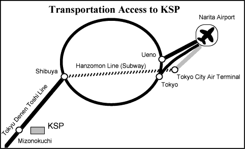
Kanagawa Science Park (KSP) is located at Kawasaki-city, Kanagawa Prefecture, which can be reached in about 30 minutes from downtown area of Tokyo and in 2 hours from Narita Airport. The nearest train station is "Mizonokuchi Station" (approximately 20 minutes from Shibuya Station of Tokyu Den-en Toshi Line) . KSP is 12 min. walk from Mizonokuchi station. available from the station.
Further Information:
For further information, please contact:
- http://vcsel-www.pi.titech.ac.jp/coesympo.html
- Symposium Secretary
Prof. F. Koyama, P&I Lab., Tokyo Institute of Technology
4259 Nagatsuta, Midori-ku, Yokohama 226-8503
Email: koyama@pi.titech.ac.jp
Tel: +81-45-924-5068, Fax: +81-45-924-5961
|
 |