| Research Facilities |
|
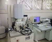
PL Photoluminescence mapping system |
|
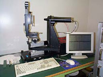
C-V Carrier density profiling system |
|
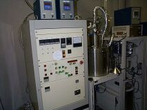
Sputter Full-automatic sputtering system for the formation of electrical insulator material, such as SiO2, for optoelectric devices. |
|
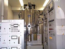
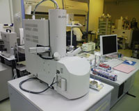
ICP Dry etching system based on inductively coupled plasma for micro-fine patterns and smooth vertical walls of lightwave integrated circuits and optical devices. |
|
EB Evaporation |
|
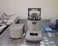
Oxidation Self-designed AlAs selective oxidation system for fabricating current confinement in VCSELs. |
|
Photo-lithography |
|
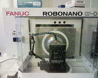
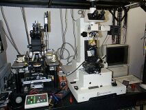
Robonano NC machine for nano-scale structure fabrication using lathe with five super precision axes. |
|
FIB |
|
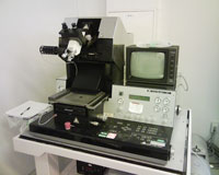
Ellipsometer |
|
AFM Atomic force scanning microscope (AFM) for observing quantum dots, epitaxial surface and micro-apertures. |
|
SEM |
|
VCSEL measurement Laser characterization system for 2-dimensional VCSEL array. |
|
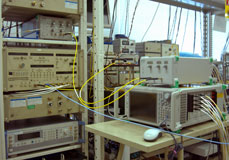
BER High speed (up to 40Gb/sec) bit error rate measuring system for lightwave communication. |
|
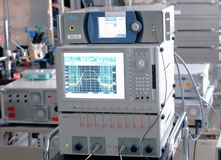
Optical network analyzer The optical network analyzer is used for measuring chromatic dispersion of an optical filter and a dispersion compensator consisting of a waveguide, dielectric multilayer, and so on. |
Copyright (C) 2011 Koyama, Uenohara, Miyamoto Lab. All rights reserved.